Samsung EUV semiconductor factory has started mass production of 7nm / 6nm process technology chips, and can also produce 3nm level in the future
February 24,2020Samsung announced that the V1 factory in Hwaseong, Gyeonggi-do, Korea has started mass production of 7nm 7LPP and 6nm 6LPP processes, which is also the world's first foundry specifically for EUV extreme ultraviolet lithography.

According to reports, Samsung's 7LPP and 6LPP processes mainly produce advanced mobile SoC chips, which have been shipping in succession this quarter. Specific customers have not been disclosed, but it seems that 7LPP will be the main force for external foundry, and 6LPP may be Samsung's own use, or only Specific customers.

According to Samsung, 6LPP can increase the transistor density by about 10% and reduce power consumption compared to 7LPP, but they are compatible with each other. IPs designed for the 7LPP process can be directly reused, which greatly reduces costs.

On the roadmap, Samsung also plans more advanced processes such as 5LPE, 4LPE, 3GAE, 3GAP, etc., which will use EUV extreme ultraviolet lithography. Among them, 5nm and 4nm can be regarded as a deep upgrade of the 7nm process, and 3nm is a new design.

Qualcomm's just-released third-generation 5G baseband Snapdragon X60 will be manufactured using Samsung's 5nm process. 3nm will be developed this year, giving up the FinFET transistor architecture that has been in use for many years.
Samsung V1 factory started construction in February 2018, and trial production will begin in the second half of 2019. In the future, capacity will be expanded rapidly. By the end of this year, the total capacity of 7LPP EUV and updated processes will be three times that of the end of last year, and the cumulative investment will also reach 6 billion. US dollars.
Hot News
-
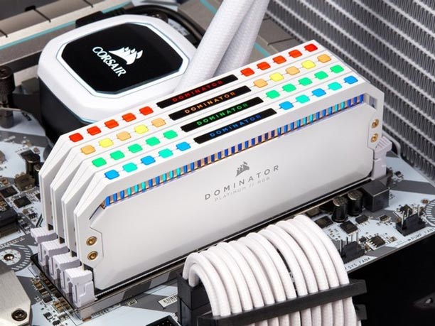
American pirate ship launches white special edition Dominator Platinum White RGB white gold ruler memory
CORSAIR who is obsessed with white today released Dominator Platinum White RGB white special edition memory which belongs to the famous platinum ruler family
-
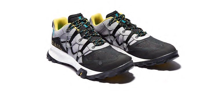
Recycled material: Timberland new outdoor city shoes GARRISON official website $120
Timberland is very accomplished in the outdoor industry The most classic rhubarb boots have always been loved by stars from all walks of life and later became well known to the public It was once out of stock and even increased in price to be bought
-
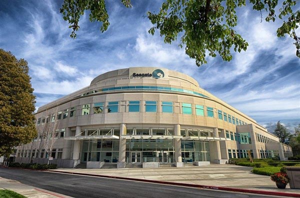
Committed to curbing the new crown epidemic: Seagate freely opens all technical patents for the prevention and treatment of new crown virus
The momentum of the new crown epidemic has not been completely contained and all parties are still making unremitting efforts to prevent and control it